 Image 1 of 4
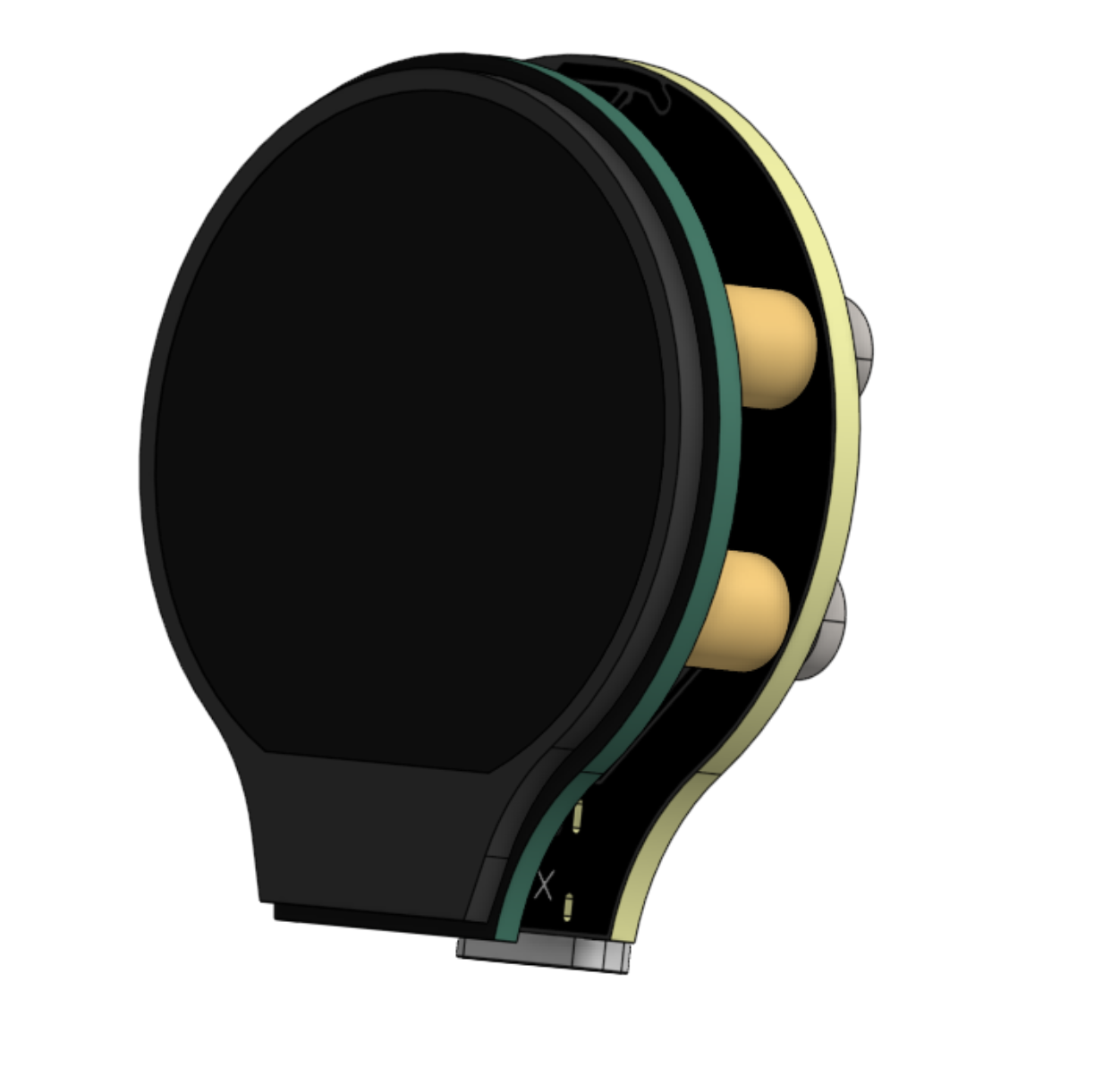 Image 2 of 4
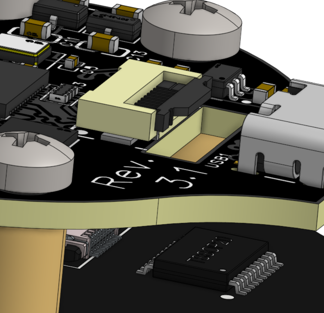 Image 3 of 4
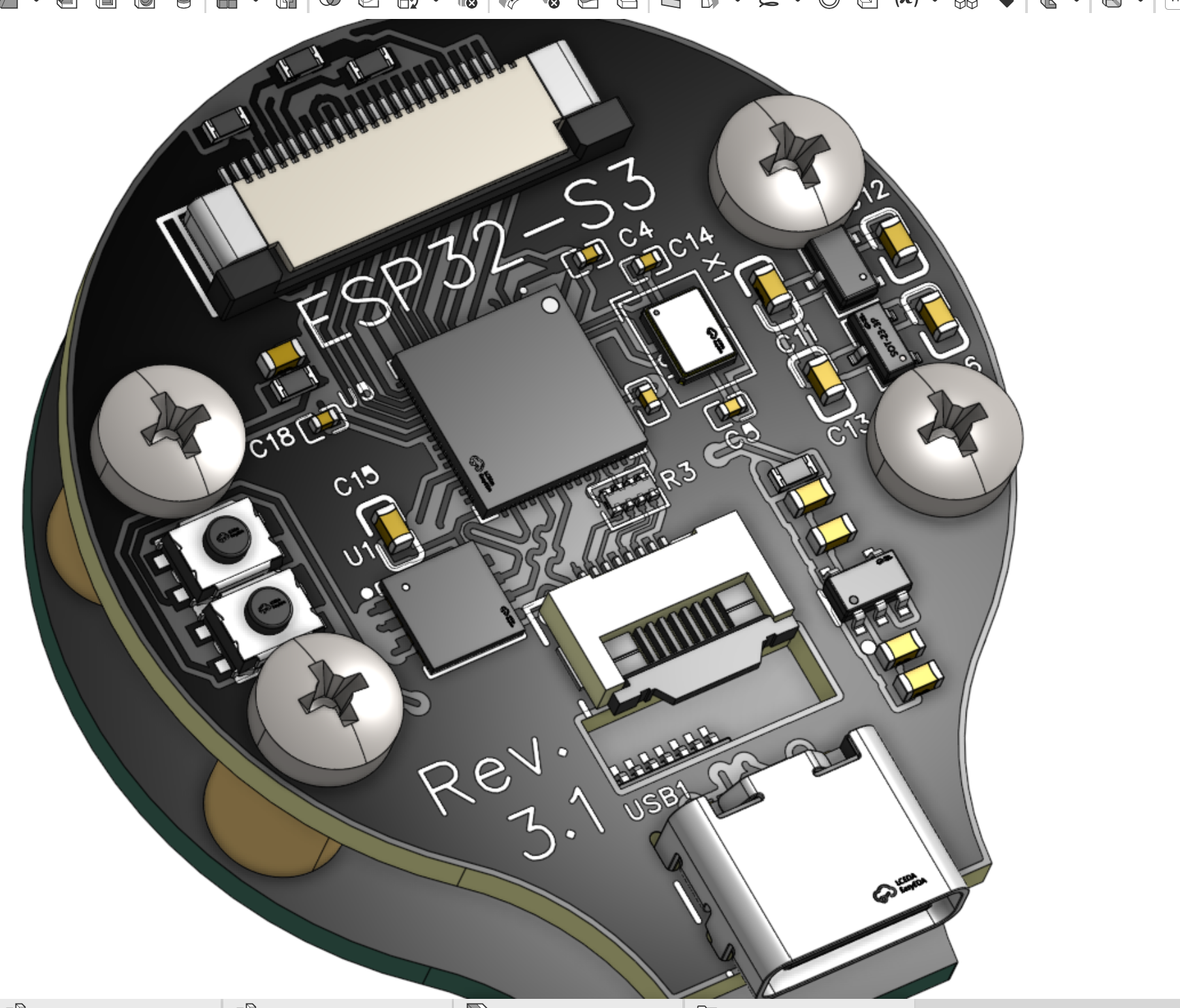 Image 4 of 4
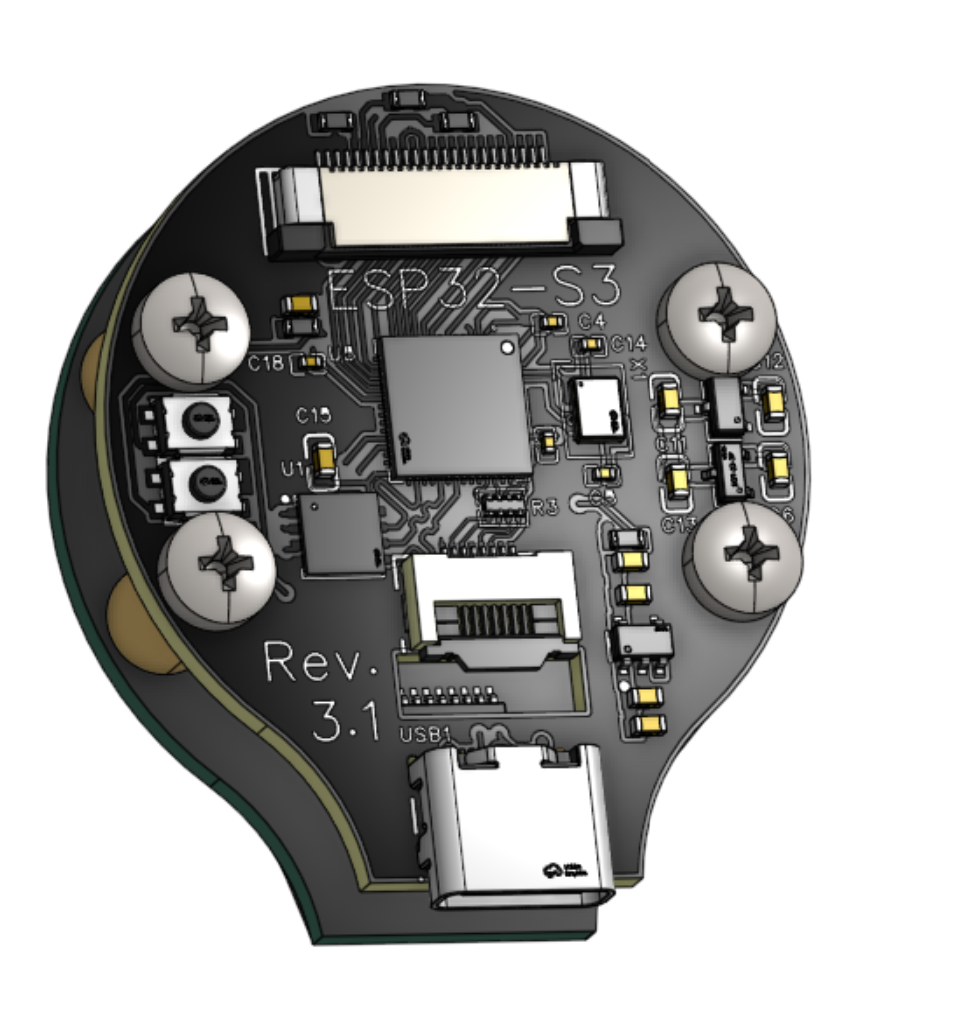
Custom PCB mounts directly to the back of the GC9A01 display module and directly connects via a built in ribbon cable to deliver maximum data throughput, an 80 MHz SPI clock with its ± 0.5 thousandths of an inch length matching enables measureable, real-world performance of 80 to 86 FPS and end-to-end latency as low as 20 ms when paired with an OV7725 camera.
Key features
Direct bolt-on design: PCB bolts to the back of the GC9A01 display for a compact, mechanically robust assembly with minimal signal path length.
High-speed SPI interface: Supports an 80 MHz SPI clock to maximize data rate and minimize transfer time.
Ribbon-cable connection: High speed, low-profile connection between display and board for easy integration into tight housings with no mess.
ESP32 S-3 Module Dual-core architecture, the module’s dual cores to divide processing tasks—one core for camera capture and preprocessing, the other for display output and higher-level logic—reducing wasted clock cycles and improving responsiveness.
DMA-driven transfers: Direct Memory Access is used extensively for camera-to-framebuffer and framebuffer-to-SPI transfers, removing CPU bottlenecks and enabling stable high-fps operation.
Optimized for OV7725: data path tuned for the OV7725 camera sensor to achieve best-case results: measured at 80 - 86 FPS and approximately 20 ms pipeline latency in real-world conditions.
Stable, deterministic performance: Combining dual-core task separation with DMA and an 80 MHz SPI link produces consistent framerates and low jitter under load.
Typical performance (real-world measured)
Frame rate: Up to 86 frames per second with OV7725 capture pipeline.
Latency: Down to ~20 milliseconds end-to-end (camera exposure → processing → display update) in optimized configurations.
Stability: Maintains high FPS under continuous operation due to DMA offload and balanced core utilization.
Technical considerations
Sensor settings: Achieving peak FPS and lowest latency requires OV7725 configured for minimal exposure, reduced vertical blanking, and an appropriate pixel clock to match the processing pipeline.
Firmware architecture: Realizing these gains requires firmware that explicitly partitions capture and display tasks across the S-3’s cores and orchestrates DMA descriptors to avoid copying or CPU wait states.
Module is not ESD protected so ensure proper handling to prevent damage to the display, the core, or surrounding componenents.
Included with the board
Custom PCB with connector footprint for GC9A01 display
Ribbon cable for display connection
firmware DMA setup for OV7725 camera and GC9A01 display
Example configuration of wiring for power, grounding, and ribbon cable routing